VT-S1080
PCB Inspection System
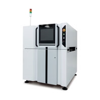
Innovating manufacturing through Omron advanced inspection technology
Related Contents
- Features
- Lineup
- Specifications
- Dimensions
- Catalog / Manual / CAD / Software
last update: April 14, 2026
Hardware configuration / Functional specifications
| Type | VT-S1080-
V3-R10 |
VT-S1040-
V3-R10 |
VT-S1080-
V3-R12 |
VT-S1040-
V3-R12 |
VT-Z600-
V3-R12 |
|
|---|---|---|---|---|---|---|
| Outer dimentions | 1180(W) × 1450(D) × 1500(H)mm (excluding tower lamp and monitor) | |||||
| Weight | Approx. 1240Kg | |||||
| Power supply | 200 to 240 V AC (Single phase); Voltage fluctuation range ±10% 50/60Hz | |||||
| Rated power | 2.0 kVA (Maximum current 10 A) | |||||
| Line height | 900±20mm | |||||
| Air supply | Not required | |||||
| Operating temperature
range |
10~35℃ | |||||
| Operating humidity
range |
35 to 80% RH (Non-condensing) | |||||
| Camera | Direct | 25Mpix | ||||
| Oblique | 5Mpix | - | 5Mpix | - | - | |
| Resolution | Direct | 10μm | 12.5μm | |||
| Oblique | 10μm | - | 10μm | - | - | |
| FOV | Direct | 51.2 × 51.2mm | 52.5 × 52.5mm | |||
| Oblique | 25.9 ×
19.4mm |
- | 25.9 ×
19.4mm |
- | - | |
| Inspection principle | Hybrid
3DShape reconstruction MDMC*12 illumination+ Phase shift (MPS*13) |
Hybrid
3DShape reconstruction MDMC*12 illumination+ Phase shift (MPS*13 option) |
Hybrid
3DShape reconstruction MDMC*12 illumination+ Phase shift (MPS*13) |
Hybrid
3DShape reconstruction MDMC*12 illumination+ Phase shift (MPS*13 option) |
2.5D Shape
reconstruction MDMC*12 illumination |
|
| Supported
PCB size |
Size | Single lane: 50(W) × 50(D)~510(W) × 680(D)mm
Dual lane: 50(W) × 50(D)~510(W) × 330(D)mm |
||||
| Thickness | 0.4~4mm | |||||
| Weight | 4Kg | |||||
| Clearance | Clearance on PCB: 50mm from board surface
Clearance under PCB: 50mm from the back of the board (including PCB warpage, deflection, component tolerance, etc.) |
|||||
| Height measurement
range |
25.4mm | - | ||||
| Inspection item | Component height, lift, tilt, missing or wrong component, wrong polarity,
flipped component, OCR inspection, 2D code, component offset (X/Y/rotation), fillet*14 (height/length, end joint width, wetting angle, side joint length), exposed land, foreign material, land error, lead offset, lead posture, lead presence, solder ball, solder bridge, distance between components, component angle |
Missing or wrong
component, wrong polarity, flipped component, OCR inspection, 2Dcode, component offset (X/Y/rotation), fillet (height/length, end joint width, wetting angle, side joint length)*14, exposed land, foreign material, land error, lead offset, lead posture, lead presence, solder ball, solder bridge, distance between components, component angle |
||||
*12. MDMC: Multi Direction/Multi Color
*13. MPS: Micro Phase Shift
*14. Post-reflow process only
last update: April 14, 2026